


From data set to tested circuit board: all manufacturing steps take place under one roof at our site in Lamspringe. Mechanical, photochemical, chemical and thermal processes work hand in hand, continuously optimised and extended with new technologies. This is how we manufacture for your current and future requirements.
- 1 Preparation
- 2 Lamination and drilling
- 3 Patterning
- 4 Surface and contour
- 5 Testing
- Process control and environment
Phase 1
Preparation
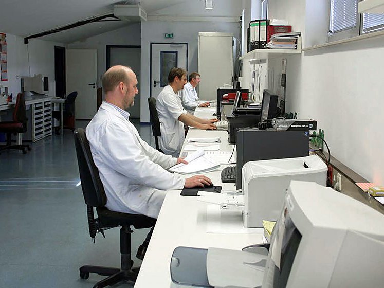
01CAM engineering – CAD/CAM
Our CAM engineering team turns your data into a product that is ready for manufacturing.
- Design rule check
- Panel layout in Hotoprint standard formats and individual process routing
- Manufacturing data for CNC, AOI and electrical test
- Process parameters for lamination, plating and etching
- Film plots for the lithographic processes
Phase 2
Lamination and drilling
02Multilayer lamination
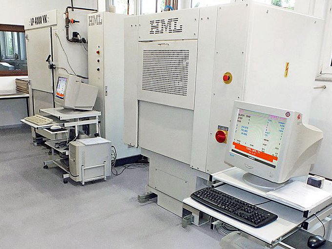
According to the build-up plan, the AOI-inspected inner layers are fixed in the press tooling together with prepregs, copper foils and press pads, and laminated in HML vacuum presses at high temperature and pressure. All press parameters are continuously monitored and documented.
03Drilling
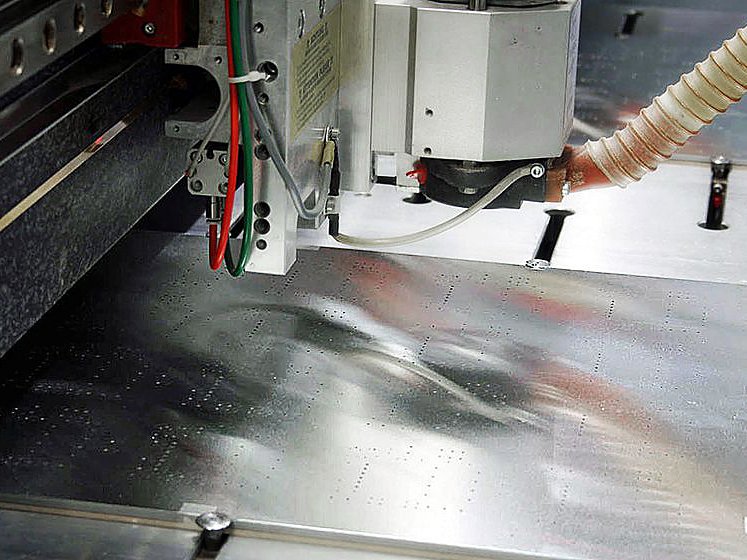
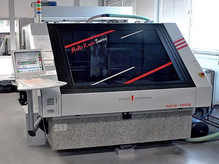
- Schmoll MX2 drilling machines with synchronous drilling spindles: high torque and high speed
- Mechanical drilling from 150 µm diameter
- 3,600 tools, continuously monitored and replaced as required
- Contact drill technology with depth measurement for precise blind vias
- Automatic loading and unloading for 24-hour operation
04Desmear, brushing and Shadow process
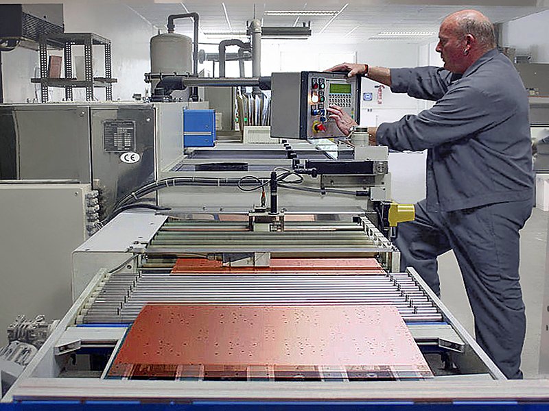
- Desmear: chemical cleaning and conditioning of the hole walls, removes resin smear and glass fibre residues
- Brushing: oscillating and rotating brush rollers deburr, ultrasound and high-pressure water clean the holes
- Shadow process: conductive graphite is deposited on the hole walls in horizontal flood baths, the basis for uniform through-hole plating
Phase 3
Patterning
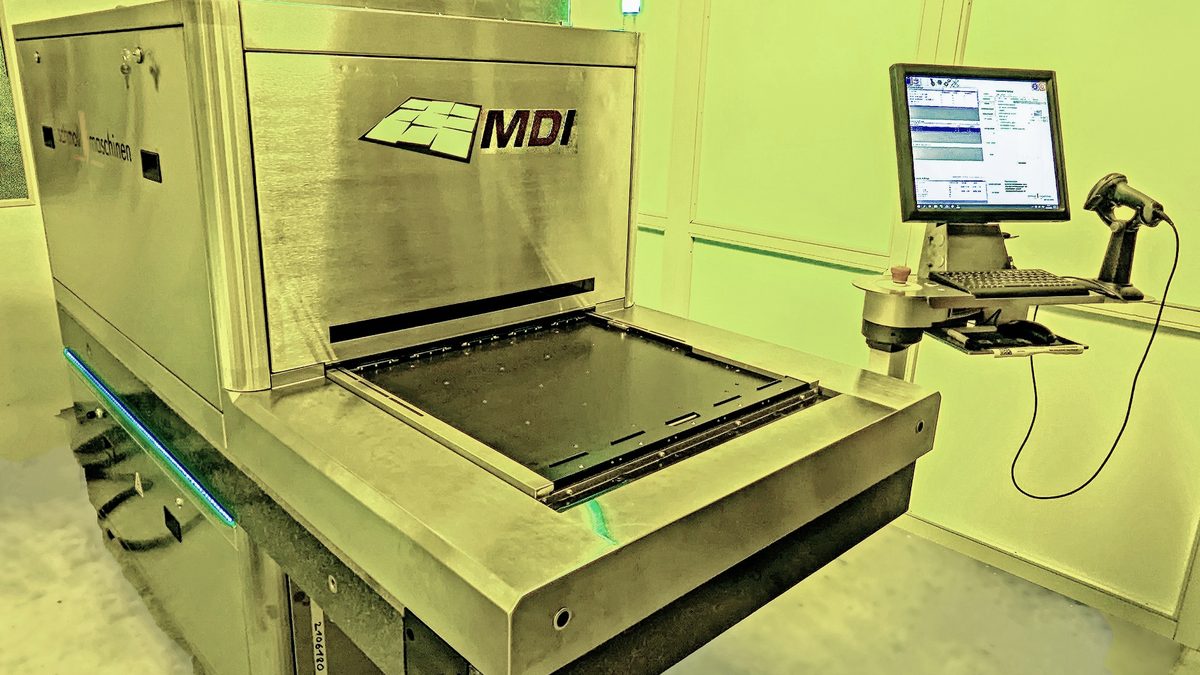
05Imaging – conductor pattern
- Lamination with photoresist in the HAKUTO cut-sheet laminator
- Digital UV exposure in the Schmoll MDI direct imaging system with more than 2 million individually controllable micromirrors and a UV LED system
- Temperature, humidity and dust particles are permanently monitored by an air-conditioning and air-purification system
06Plating
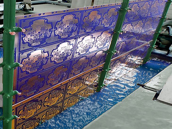
- Electrolytic copper deposition on tracks, areas and vias according to customer specification, typically 40–50 µm or 105 µm outer copper and 25 µm in the hole wall
- Pure tin as etch resist
- MMS coating thickness measurement: release only when the specifications are met, results are documented
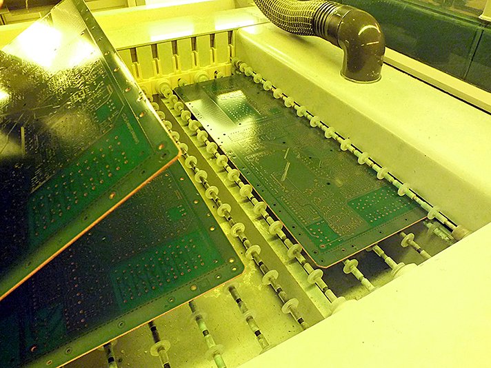
07Stripping and etching
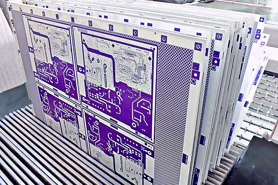
After the photoresist has been removed, an alkaline etchant dissolves the exposed base copper. The tin protects the conductor pattern and is then removed in the tin stripping process.
08Optical inspection – AOI
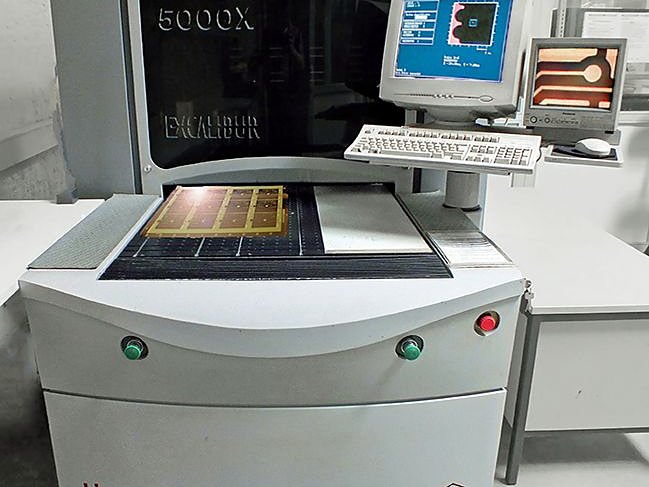
- Automated optical inspection against the CAD data: track widths and spacing, short circuits and open circuits
- Also detects hidden defects such as track constrictions that are hardly noticeable in electrical testing
- All inner layers are inspected before lamination
- Cross-sections document metal deposition and inner layer connection
Phase 4
Surface and contour
09Solder mask
- Pre-treatment with the MEC etch bond process for a micro-rough surface with optimum adhesion
- Applied by curtain coating, thickness according to specification
- Standard green, other colours on request
- UV exposure (Bacher Systems) with automatic camera registration, developing and infrared drying
- Solder mask systems exclusively from Peters
10Surface finishing
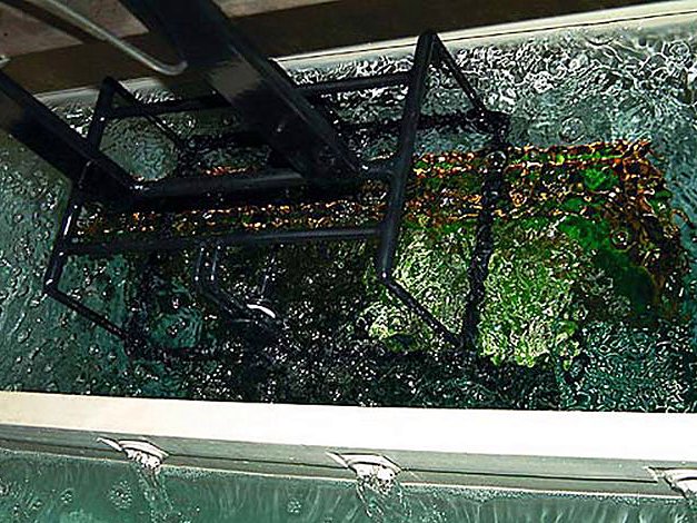
Final finishes for pads and holes:
- Hot air levelling (HAL) lead-free with SN100CL solder (BALVER), leaded for applications exempt from RoHS
- Electroless nickel-gold
- Immersion tin
- Other finishes on request, see technical data
11Milling
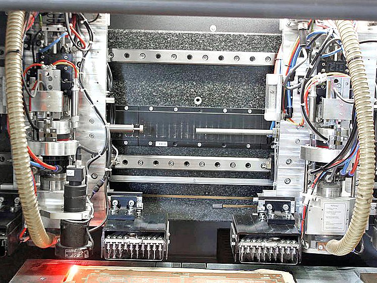
- Schmoll MX series with CCD camera system
- Positioning accuracy ±15 µm via optically detected fiducials
- Outer contours, internal cut-outs and complex shapes
- Step and depth milling for flex, rigid-flex and semi-flex
12Screen printing
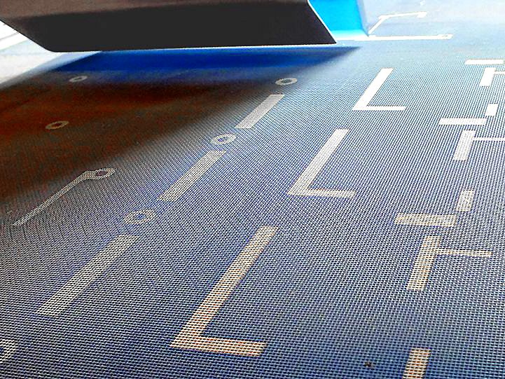
- Legend print, via filling, peelable mask and carbon printing
- Screens with suitable mesh count, all stencils made in-house
- Photosensitive inks with UV exposure for the finest structures
- Ink systems from Peters
Phase 5
Testing
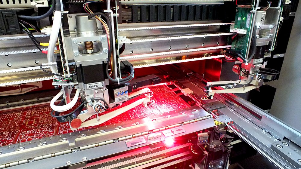
13Electrical testing
Finally, we electrically test every circuit board against the netlist from your CAD data.
- Flying probe tester (ATG A5 neo) for prototypes and small batches: no test fixture required, quickly set up
- Fixture testing for large series: high test density and speed, in cooperation with ETZ, a local test service provider
Process control and environment
- All processes are continuously monitored, documented and controlled, equipment and measuring systems are regularly calibrated
- Our own laboratory for analysing the chemical processes
- Our own wastewater treatment plant: cleaning, neutralisation and treatment before discharge
- Avoiding waste, recycling residues properly
- Economical use of raw materials, energy and water, heat recovery from process waste heat
We will be happy to show you what is possible for your project.