


Quality is not something that only happens at the end. Every circuit board is inspected, measured and documented, from the incoming inspection of the base material to delivery, in our own laboratory and with state-of-the-art testing systems.
- Incoming inspection and laboratory
- Optical inspection
- Cross-section analysis
- Electrical testing
- Marking and documentation

Inspection area 1
Incoming inspection and laboratory
01Incoming goods inspection
Base materials and chemicals are inspected on arrival, before they go into production.
02Chemical laboratory control
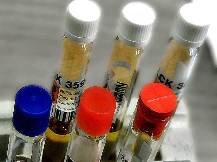
- Our own on-site laboratory for analysing all chemical processes
- Process baths are continuously monitored and controlled
- Equipment and measuring systems are regularly calibrated and maintained
03MMS coating thickness measurement
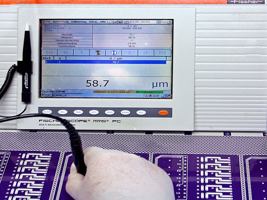
- Measurement of the copper thickness after plating with the FISCHERSCOPE® MMS®
- Release for further processing only when the specifications are met
- All measured values are documented
Inspection area 2
Optical inspection
04AOI – automated optical inspection
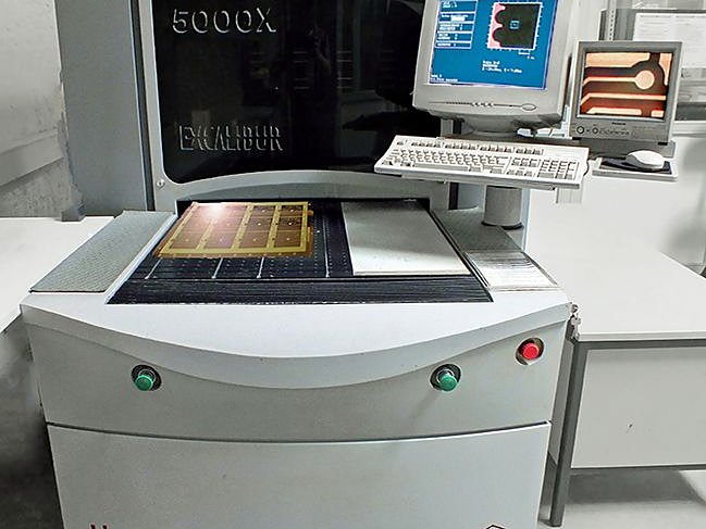
- Comparison of the conductor pattern with your CAD data
- Inspection of track widths and spacing, short circuits and open circuits
- Also detects hidden defects such as track constrictions
- All inner layers are inspected before lamination
05Visual inspection
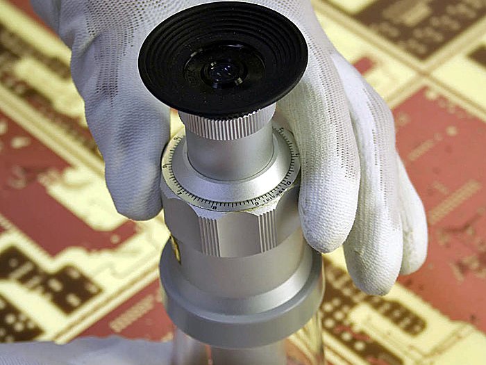
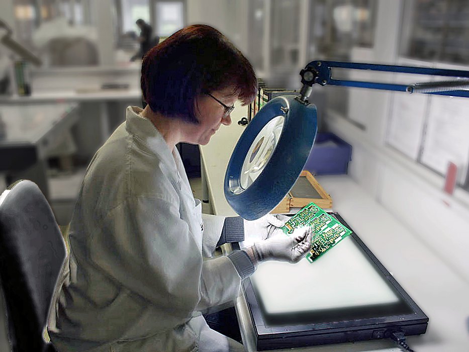
- Visual inspection by trained staff
- Inspection of surface finish, solder mask and printing
- Outgoing and final inspection before shipping
Inspection area 3
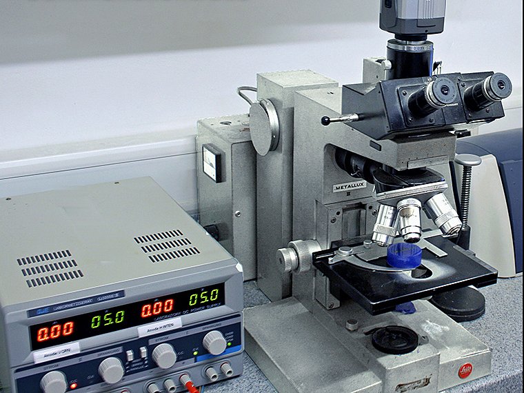
Cross-section analysis
06Metallisation and plated through-holes
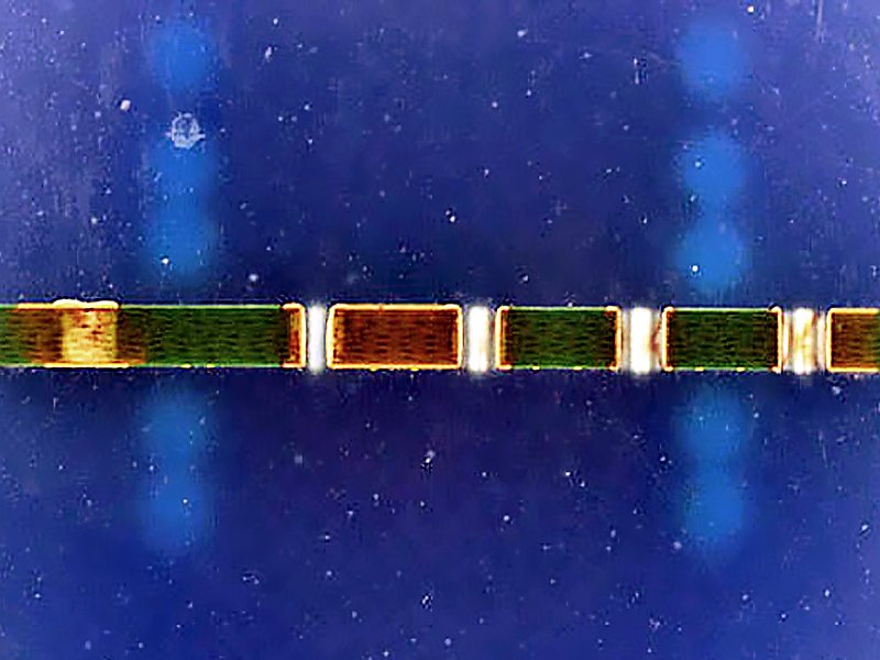
In a cross-section (microsection), the circuit board is examined under the microscope. This is how we monitor and document the quality of the metal deposition and the connection of the inner layers, including in the holes.
07Layer thicknesses in detail
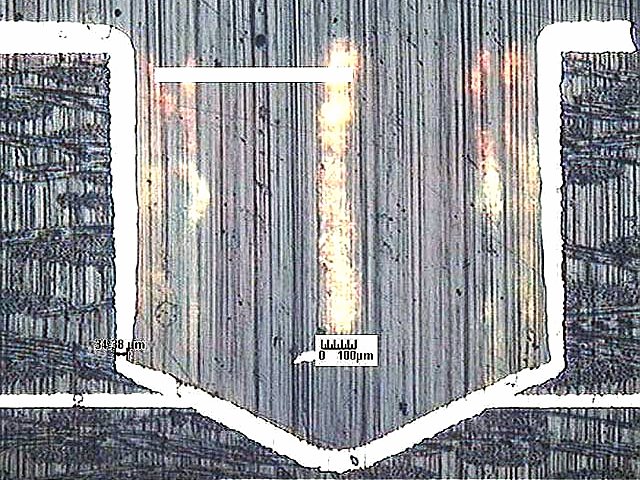
Copper thicknesses in the hole wall and in blind vias are measured directly in the cross-section and recorded.
Inspection area 4
Electrical testing
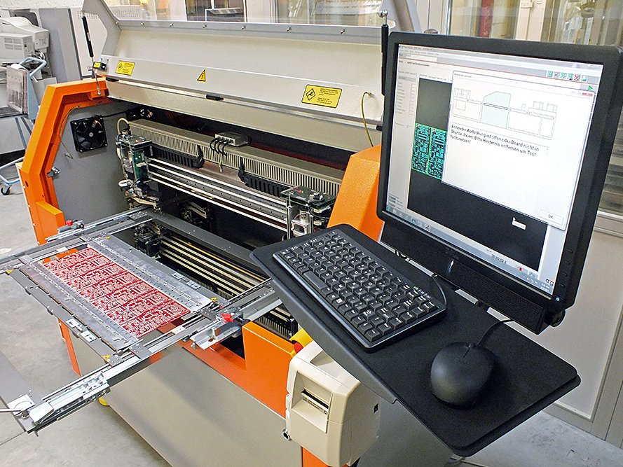
08Flying probe
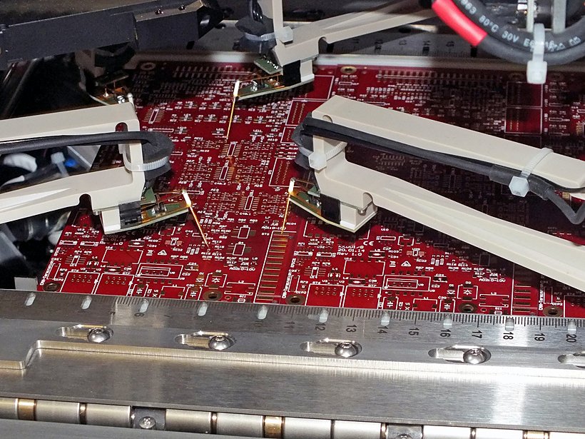
- Every circuit board is tested against the netlist from your CAD data
- ATG A5 neo flying probe tester for prototypes and small batches
- No test fixture required, quickly set up for new products
09Fixture testing for series production
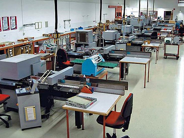
- High test density and speed for large quantities
- In close cooperation with ETZ, a local test service provider
Marking and documentation
- Date and batch marking on request, applied with the MDI exposure system, in the solder mask or in the legend print
- UL marking on request
- Test report on request
- First article inspection report (FAI) and extended test reports on request
- All process and measurement data are documented and traceable
Get in touch – we will agree the scope of testing and documentation with you.