


The key manufacturing limits and design rules at a glance, for single-sided, double-sided, multilayer, flex and rigid-flex PCBs. Limit values do not all apply in every combination at the same time. For demanding designs, we are happy to check your data in advance.
Datasheet as PDF (German) As of November 2026
- Conductor pattern
- Holes and vias
- Sizes and thicknesses
- Milling and tolerances
- Solder mask and printing
- Surface finishes
- Materials and certificates
Conductor pattern
| Outer layers | Inner layers | |
|---|---|---|
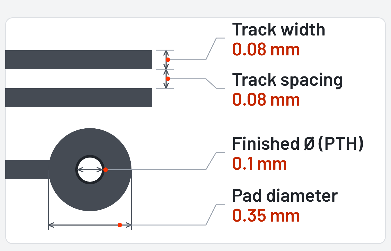
| Min. track width | 0.08 mm | 0.08 mm |
| Min. track spacing | 0.08 mm | 0.08 mm |
| Min. pad diameter | 0.35 mm | 0.35 mm |
| Min. SMD pad | 0.2 mm |
| Min. component spacing | 0.37 mm |
Holes and vias
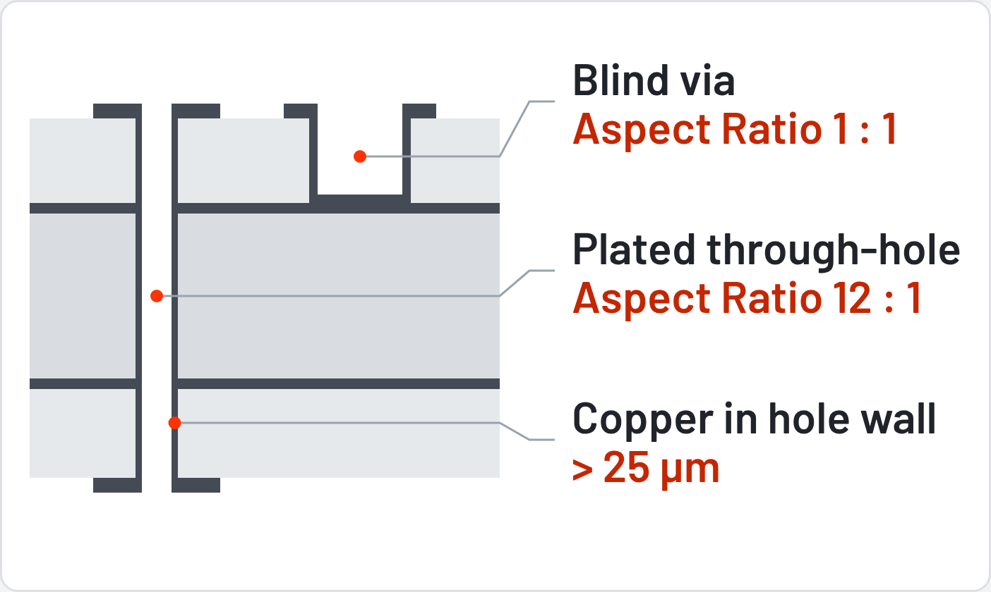
| Aspect ratio (hole depth to min. Ø) | 12 : 1 |
| Min. finished hole diameter (PTH) | 0.1 mm |
| Mechanically drilled microvias | 0.1 – 0.2 mm |
| Blind via – min. finished diameter | 0.2 mm |
| Blind via – min. pad diameter outer / inner | 0.35 mm |
| Blind via – aspect ratio | 1 : 1 |
| Copper in the hole wall | > 25 µm |
Sizes and thicknesses
| Layer count | up to 12 layers |
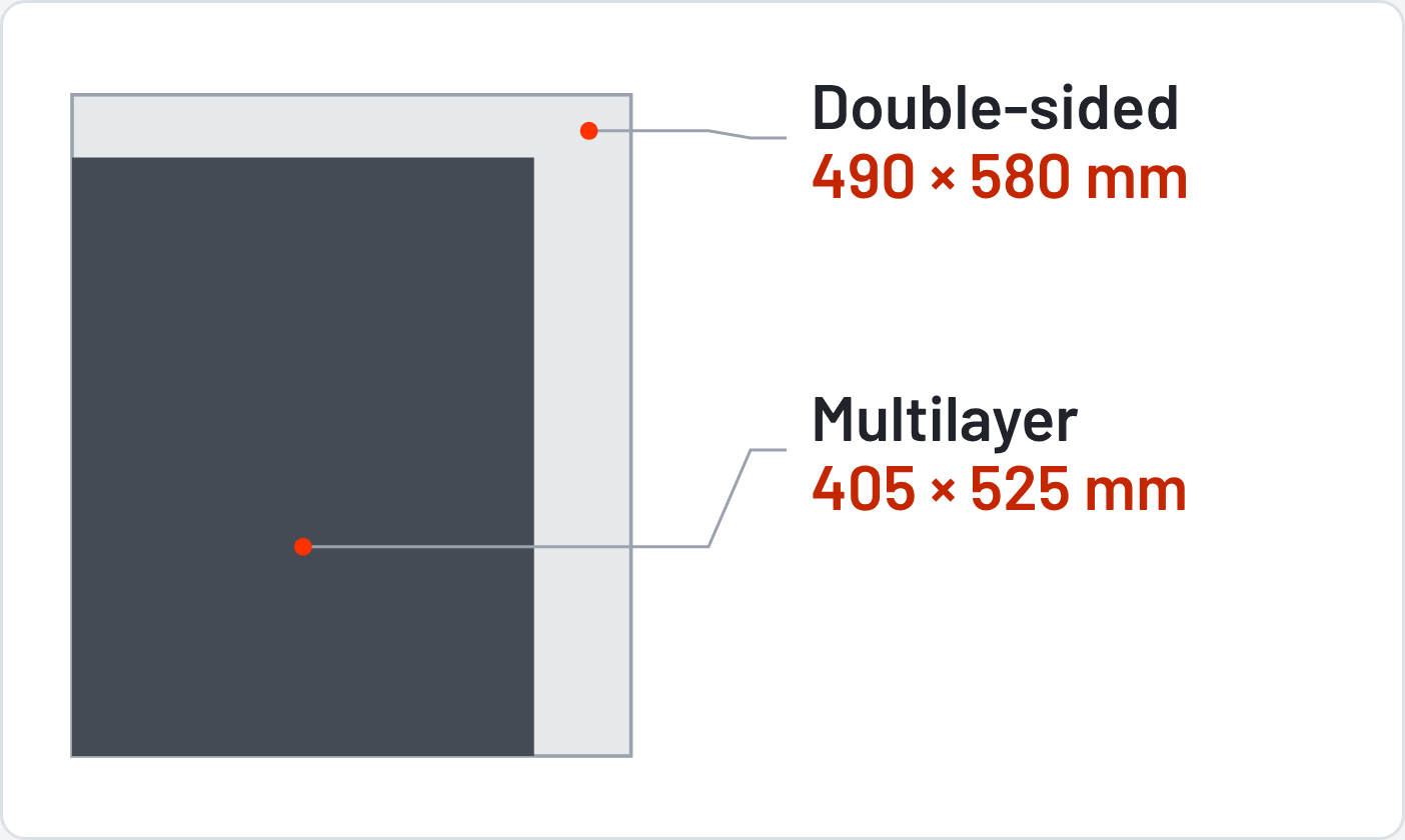
| Max. size double-sided | 490 × 580 mm |
| Max. size multilayer | 405 × 525 mm |
| Final PCB thickness | 0.1 – 3.5 mm |
| Min. layer spacing | 0.05 mm |
| Standard final copper | 35 / 70 µm |
| Copper thickness | 9 – 235 µm |
Milling and tolerances
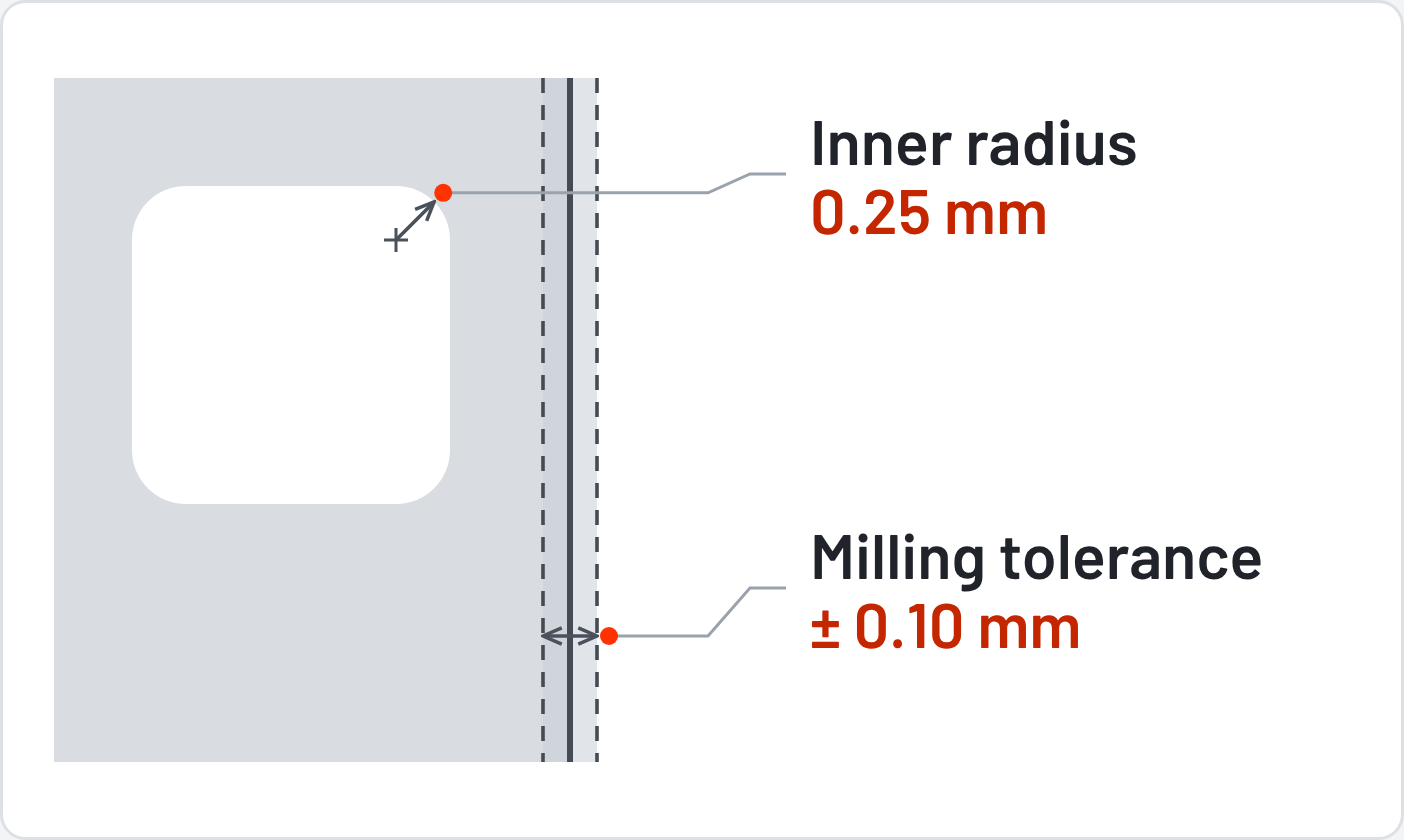
| Min. inner radius | 0.25 mm |
| Milling tolerance | ± 0.10 mm |
| V-scoring – min. material thickness | 0.5 mm |
| Tolerance PTH diameter | +0.10 / –0.05 mm |
| Tolerance hole position | ± 0.05 mm |
| Tolerance base material thickness | ± 10 % |
Solder mask and printing
| Solder mask – min. clearance | 0.05 mm |
| Peelable mask – min. overlap | 0.3 mm |
| Peelable mask – min. clearance | 0.6 mm |
Solder mask – colours
- Green
- Red
- White
- Black
- Blue
Special printing
- Peelable mask, RoHS-compliant
- Carbon printing
All solder masks and inks we use are supplied by Lackwerke Peters.
Surface finishes
- HAL / lead-free HAL
- Electroless nickel immersion palladium immersion gold (ENIPIG)
- Electroless nickel immersion gold (ENIG)
- Electroplated nickel-gold
- Gold-plated edge connectors
- Immersion tin
- OSP
Materials and certificates
Base materials
- All FR4*
- Polyimide**
- Rogers®**
- Aluminium, copper-clad**
* For UL-marked PCBs, FR4 base materials and solder masks are restricted
** Without UL marking
Certifications
- DIN EN ISO 9001:2015
- UL certification (US and C) for ZPVM2 and ZPVM8, E-File E119015
- ZPVM8 is recognised by CSA
You can find our certificates in the download area.
Is your design at the limit of what is feasible?
Send us your data – we will check feasibility in advance.